- 您现在的位置:买卖IC网 > Sheet目录510 > SI4731-D50-GM (Silicon Laboratories Inc)IC RADIO RECEIVER AM/FM 20-QFN
Si4730/31-D50
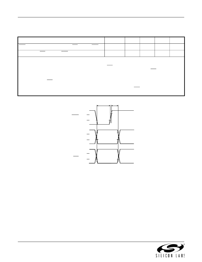
Table 4. Reset Timing Characteristics 1,2,3
(V A = 2.7 to 5.5 V, V D = 1.62 to 3.6 V, T A = –20 to 85 °C)
Parameter
RST Pulse Width and GPO1, GPO2/INT Setup to RST ? ?
GPO1, GPO2/INT Hold from RST ?
Symbol
t SRST
t HRST
Min
100
30
Typ
—
—
Max
—
—
Unit
μs
ns
Important Notes:
1. When selecting 2-wire mode, the user must ensure that a 2-wire start condition (falling edge of SDIO while SCLK is
high) does not occur within 300 ns before the rising edge of RST.
2. When selecting 2-wire mode, the user must ensure that SCLK is high during the rising edge of RST, and stays high until
after the first start condition.
3. When selecting 3-wire mode, the user must ensure that a rising edge of SCLK does not occur within 300 ns before the
rising edge of RST.
4. If GPO1 and GPO2 are actively driven by the user, then minimum t SRST is only 30 ns. If GPO1 or GPO2 is hi-Z, then
minimum t SRST is 100 μs, to provide time for on-chip 1 M ? devices (active while RST is low) to pull GPO1 high and
GPO2 low.
t SRST
t HRST
RST
GPO1
GPO2/
INT
70%
30%
70%
30%
70%
30%
Figure 1. Reset Timing Parameters for Busmode Select
6
Rev. 1.0
发布紧急采购,3分钟左右您将得到回复。
相关PDF资料
SI4737-C-EVB
BOARD EVAL SI4737 VERSION C
SI4743-C-EVB
BOARD EVALUATION FOR SI4743-C
SI4770-A-EVB
BOARD EVAL FOR CE AM/FM SI4770
SI4777-A20-GM
IC RCVR AM/FM CE HD-RADIO TUNER
SI4804CDY-T1-E3
MOSFET 2N-CH 30V 8A SO8
SI4808DY-T1-GE3
MOSFET N-CH/SCHOTTKY 30V 8SOIC
SI4812BDY-T1-GE3
MOSFET N-CH D-S 30V 8-SOIC
SI4814BDY-T1-GE3
MOSFET N-CH/SCHOTTKY 30V 8SOIC
相关代理商/技术参数
SI4731-D50-GMR
制造商:Silicon Laboratories Inc 功能描述:ADVANCED AM/FM RDS RECEIVER FOR MOBILE DEVICES - Tape and Reel 制造商:Silicon Laboratories Inc 功能描述:IC RADIO RECEIVER AM/FM 20-QFN 制造商:Silicon Laboratories Inc 功能描述:MOBLE DEV AM/FM/RCVR RDS 3X3X0.55 20P
SI4731-D60-EVB
功能描述:BOARD EVALUATION FOR SI473-D60 RoHS:是 类别:RF/IF 和 RFID >> RF 评估和开发套件,板 系列:- 标准包装:1 系列:- 类型:GPS 接收器 频率:1575MHz 适用于相关产品:- 已供物品:模块 其它名称:SER3796
SI4731-D60-GM
功能描述:IC RADIO RX AM/FM/AUX 20QFN RoHS:是 类别:RF/IF 和 RFID >> RF 接收器 系列:- 产品培训模块:Lead (SnPb) Finish for COTS 产品变化通告:Product Discontinuation 09/Jan/2012 标准包装:50 系列:* 频率:850MHz ~ 2.175GHz 灵敏度:- 数据传输率 - 最大:- 调制或协议:- 应用:* 电流 - 接收:* 数据接口:PCB,表面贴装 存储容量:- 天线连接器:PCB,表面贴装 特点:- 电源电压:4.75 V ~ 5.25 V 工作温度:0°C ~ 85°C 封装/外壳:40-WFQFN 裸露焊盘 供应商设备封装:40-TQFN-EP(6x6) 包装:托盘
Si4731-D60-GMR
功能描述:射频接收器 BRDCAST AM/FM/AUXIN RADIO RECEIVER/RBDS RoHS:否 制造商:Skyworks Solutions, Inc. 类型:GPS Receiver 封装 / 箱体:QFN-24 工作频率:4.092 MHz 工作电源电压:3.3 V 封装:Reel
SI4731-D60-GU
功能描述:IC RADIO RX AM/FM/AUX 24SSOP RoHS:是 类别:RF/IF 和 RFID >> RF 接收器 系列:- 产品培训模块:Lead (SnPb) Finish for COTS 产品变化通告:Product Discontinuation 09/Jan/2012 标准包装:50 系列:* 频率:850MHz ~ 2.175GHz 灵敏度:- 数据传输率 - 最大:- 调制或协议:- 应用:* 电流 - 接收:* 数据接口:PCB,表面贴装 存储容量:- 天线连接器:PCB,表面贴装 特点:- 电源电压:4.75 V ~ 5.25 V 工作温度:0°C ~ 85°C 封装/外壳:40-WFQFN 裸露焊盘 供应商设备封装:40-TQFN-EP(6x6) 包装:托盘
Si4731-D60-GU2
制造商:SILABS 制造商全称:SILABS 功能描述:BROADCAST AM/FM/SW/LW RADIO RECEIVER
Si4731-D60-GUR
功能描述:射频接收器 BRDCAST AM/FM/AUXIN RADIO RECEIVER/RBDS RoHS:否 制造商:Skyworks Solutions, Inc. 类型:GPS Receiver 封装 / 箱体:QFN-24 工作频率:4.092 MHz 工作电源电压:3.3 V 封装:Reel
Si4731-Demo
功能描述:射频开发工具 Standalone Demo and Eval Board 3x3x0.55 RoHS:否 制造商:Taiyo Yuden 产品:Wireless Modules 类型:Wireless Audio 工具用于评估:WYSAAVDX7 频率: 工作电源电压:3.4 V to 5.5 V
